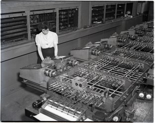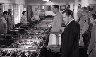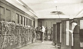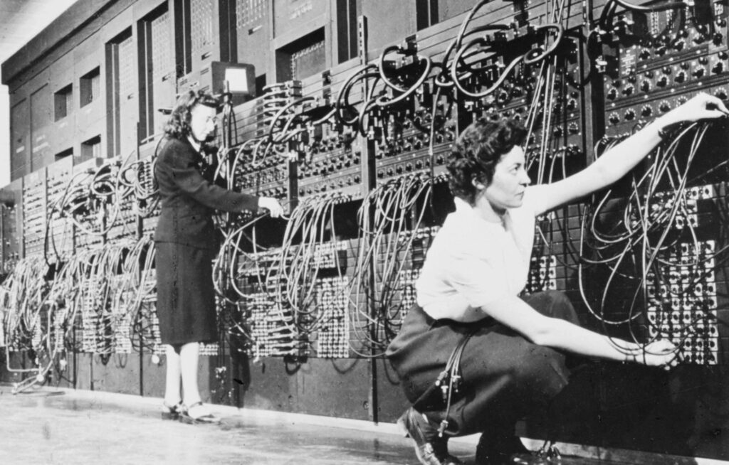
This is what it was like to program the first computer, ENIAC, introduced in 1947. Pictured are programmers Marlyn Wescoff and Ruth Lichterman. Image: American Physical Society.
By John Bamford
“The number of transistors and resistors on a chip doubles every 24 months.” — Gordon Moore
“How would you like to have most of your life’s work end up on a square centimeter of silicon?” — John Presper Eckert Jr., Co-Inventor of ENIAC
“It has today occurred to me that an amplifier using semiconductors rather than vacuum is in principle possible.” — William Shockley, Laboratory notebook, 29 Dec 1939
“My parents didn’t like me. For bathtub toys they gave me a blender and a transistor radio.” — Rodney Dangerfield
On February 14, 1946, the U.S. Army issued a press release signifying the development of ENIAC, the world’s first electronic, large-scale, programmable, general purpose digital computer.
ENIAC is the acronym for Electronic Numerical Integrator and Computer.
The press release stated, “A new machine that is expected to revolutionize the mathematics of engineering and change many of our industrial design methods was announced today by the War Department, a “mathematical robot’ working at ‘phenomenal’ speed that ‘frees scientific thought from the drudgery of lengthy calculating work.’” And what was the first “drudgery of lengthy calculating work” that ENIAC was going to free us from?
It was June 1943, and Allied forces were beginning their invasion campaigns against Nazi Germany in Europe and fighting from island to island in the Pacific against the Japanese empire. New weapons technologies were being developed and with them the pressing need for more and more accurate and reliable ballistics charts and tables; charts and tables that would significantly improve the aim of land (and sea) artillery.
Producing these charts and tables was no small accomplishment. Consider all the variables: the mass, shape and composition of the projectile; wind speed; temperature; humidity; air density; muzzle velocity; gunpowder composition and temperature. Initially this was all done using paper and pencil, with slide rules, tables, and push-button calculators to perform mathematical formulas. Eventually a mechanical computing machine was introduced, called the ‘differential analyzer’.
- A differential analyzer mechanical computing machine at the Moore School of Electrical Engineering, University of Pennsylvania. Nearly 30 feet in length and 10 feet in width with 37,761 parts which ran throughout the war on the computation of ballistics tables. University of Pennsylvania
- A “Hollywood” differential analyzer being used to translate intercepted alien messages and uncover their plot to invade Earth. “Earth vs the Flying Saucers” 1956. Columbia Pictures.
Much of the manual work done on ballistics tables and charts was by women, nicknamed “computors”.
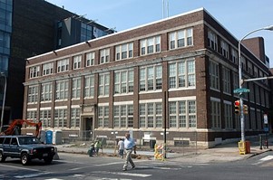
Moore School of Electrical Engineering, University of Pennsylvania. Image (Wikipedia)
Over 200 of them worked at the Moore School of Electrical Engineering at the University of Pennsylvania. A few of them were eventually selected to be “programmers” of ENIAC, and the Moore School offered the first computer course in the summer of 1946).
It was at the Moore School of Electrical Engineering that physicist John Mauchly of Ursinus College and electrical engineer John Presper Eckert Jr. first designed ENIAC as part of a proposal to the U.S. Army for the use of digital electronic signals. This technology generated, stores and processed data in positive and non-positive states, represented by 1’s and 0’s. These were conveyed using vacuum tubes to carry out mathematical calculations, producing results tremendously faster than manual methods or mechanical devices.
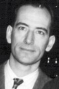
- John Mauchly (Wikipedia)
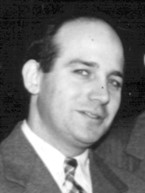
- J.(John) Presper Eckert, Jr. (Wikipedia)
- John G. Brainerd, 1966 www.archives.upenn.edu
In June 1943, under the code name “Project PX” with John Brainerd as the principal investigator and with the support of Herman Goldstine, work began on ENIAC with funding provided by the U.S. Army, Ordinance Corps, Research and Development Command.
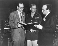
- ENIAC’s design and construction was financed by the U.S. Army, led by Major General Gladeon M. Barnes and was designed by engineers John Mauchly and J. Presper Eckert. www.penntoday.upenn.edu
- Glen Beck and Frances Snyder Holberton at the ENIAC in Ballistic Research Laboratory building 328. National Museum, United States Army
- Betty Jennings and Frances Bilas operate ENIAC’s main control panel while the machine was located at the University of Pennsylvania’s Moore School. National Museum, United States Army.
ENIAC was proposed to be electronic, programmable, high speed and general purpose.
It required a year to design and almost 2 years to build at a cost of about $500,000, which is equivalent to about $8.5 million in today’s money. It weighed 30 tons (about 27,000 kilograms), had a footprint of about 1,500 square feet, and used over 70,000 resistors, 18,000 vacuum tubes, 1,500 relays, 6,000 manual switches, 10,000 capacitors. ENIAC consumed about 174,000 watts of power with two 20 horsepower air blowers to cool it down from all the heat the components generated.
ENIAC was what we would call today “modular,” composed of individual panels, units, and modules to perform different functions. Accumulator modules could add and subtract and hold ten-digit decimal numbers in ten-position ring counters to enable 10’s complement methods. Some accumulators had special multiplier units to perform rapid multiplication operations. Some accumulators handled division functions and square root functions.
There were initiating units for starting and stopping ENIAC, a unit for synchronizing other units; a master programming unit which controlled the reading of IBM punch-cards for programming instructions. Another unit controlled a card punch machine for printing, a constant transmitter, and three function tables.
Altogether, the machine could perform approximately 500 floating-point operations, multiply two 10 digit numbers in about .0028 seconds, and perform a division or square root in about .0286 seconds. These were based on a machine cycle of about .0002 seconds, which was established by the 100 kHz the cycling clock.
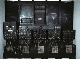
ENIAC Accumulator #2, University of Pennsylvania www.si.edu
Although ENIAC didn’t initially have a system for memory storage, it could output results to physical punch cards which were then used to input data. Results could also be printed. Eventually, in 1953, a magnetic-core memory was added. And there were tubes, tubes, and more tubes.
For example, each digit that ENIAC stored required ten-position ring counters with 36 vacuum tubes per digit. Calculations were performed by “counting” pulses with the ring counters and generating carry pulses if the counter “wrapped around”, all based on emulating the digit wheels of a mechanical adding machine.
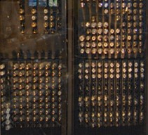
- Detail of the back of a section of ENIAC, showing vacuum tubes. The 1946 ENIAC computer used about 18,000 vacuum tubes and consumed 150 kW of power (Wikipedia)
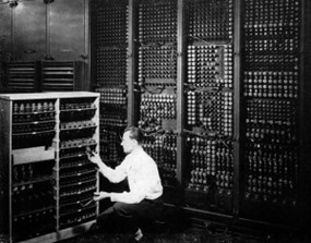
- ENIAC vacuum tube panel tube changing. U.S. Army. www.computerhistory.org
Programming ENIAC was a complex task.
First the program steps were mapped on paper, then these paper maps were translated into physical combinations of plugboard wires and hundreds of multi-position switches, a process that took days to complete.
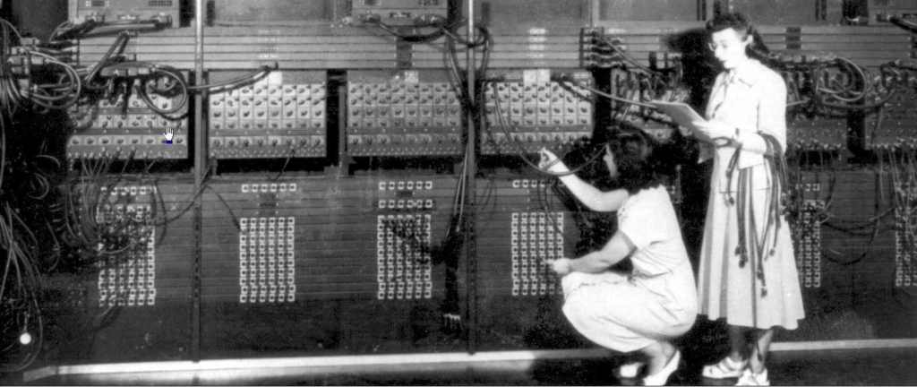
Gloria Ruth Gordon, Ester Gerston, two early ENIAC programmers (changing the wiring connections of ENIAC plugboards) at work in front of an ENIAC patch bay. Image source.
Arthur Burks was the mathematician selected to demonstrate ENIAC at the first Army Press Corps event in February 1946.
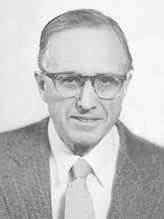
Arthur W. Burks. ScienceDirect.com
In a talk that he gave at the University of Michigan in 1974, he recalled that he first demonstrated the addition of 5,000 numbers in one second, then he demonstrated the trajectory calculation for a shell that took 30 seconds to go from gun to target. This would have taken 3 days by human “computors” and 30 minutes using a differential analyzer. ENIAC calculated this is 20 seconds! Is there any wonder why the press started referring to ENIAC as the “Giant Brain”? The movies of the time depicted giant ants, giant spiders, giant wasps, and now we had the “Giant Brain”.
From its beginnings as a ballistics calculator ENIAC went on to be used in complex calculations involved in the design of the hydrogen bomb, as well as calculations related to cosmic ray studies, wind tunnel design and even weather forecasting. This continued until early October 1955, when it was reported that a lightning strike proved fatal and it was all over for ENIAC.
It’s been said that during its operational lifetime of over 70,000 hours, ENIAC performed more calculations than all of mankind up until then. This is difficult to prove or disprove, but it makes for a great quote.
Essentially ENIAC was a collection of machines, called panels or units or modules, each doing some sort of arithmetic calculation using up to 10-digit numbers and having the ability to pass results between modules via what we now call data buses. Each of the modules on their own could send and receive numbers, perform an arithmetic calculation, hold the result ,and then be able to initiate the next modular operation.
And at its core were vacuum tubes!
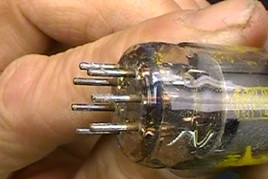
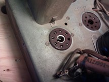
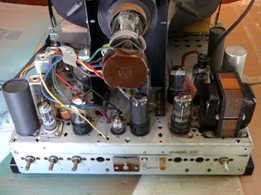
Yes those things. You remember them (maybe) from your grandparents’ first television sets. They were glowing hot, short tubes of glass, with short metal pins sticking out the bottom, sometimes with a metal pin on top. The plugged into a metal board or chassis that contained sockets with holes that matched the pins at the bottom of the tubes.
- Radio vacuum tube. www.hackaweek.com
- Radio vacuum tube plug-in socket. www.retrovoltage.com
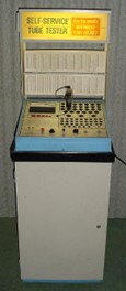
When they “burned out”, as vacuum tubes did more often than you’d expect, you would make a trip to the local hardware or corner store and use their tube tester to figure out which tube had failed and purchase a replacement (hopefully they had one!).
- Hoffman Model 7M112 Tabletop Television (1952). www.antiqueradio.org
- Eico 660 (Mercury 204) tube tester, 1969. www.diyaudio.com
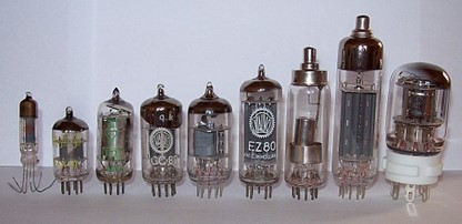
- Some example thermionic vacuum tubes, some miniature style, some with top cap connections for higher voltages. (Wikipedia)
And, while your grandparents’ old television might have had only a few tubes, each digit stored in ENIAC required 36 of these things. Vacuum tubes came in different varieties: diodes, triodes, dual triodes.
ENIAC held about 18,000 of these vacuum tubes. One or two or several of these might fail every day or two, requiring a lot of time and effort to find and replace the failed tube(s) (just imagine all of the trips to the hardware store!). But as they gained experience, engineers got better and better at tracking down the failed tubes, and improvements in engineering, materials, and construction greatly reduced the problem. Tube failures were caused by thermal stress during warm-up and cool-down times so these events were taken more slowly or through more gradual temperature changes.
And why the vacuum tube?
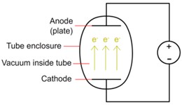
A simplified diagram of a vacuum tube (diode=2 electrodes). When the cathode is heated, and a positive voltage is applied to the anode, electrons can flow from the cathode to the anode. A separate power source is used to heat the cathode. www.engineering.com
Since digital computing relies on discrete signals, not analogue or continuous signals, and because binary methods were developed to represent any number, letter, or symbol with combinations of “0”s and “1”s, we needed a way to represent these “0”s and “1”s in a machine implementable form. And we needed ways to manipulate, process, operate on these binary representations.
We needed electronic switches that could be manipulated quickly and reliably and accurately to produce electric “signals” where an “ON” signal would represent a “1” and an “OFF” signal would represent a “0”. For that, enter the simplest vacuum tube, the diode, courtesy of English engineer John Ambrose Fleming in 1904.
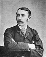
- English engineer John Ambrose Fleming, 1980. www.wikipedia.org
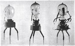
- Some of the first diodes created by John Ambrose Fleming. www.wikipedia.org

A diode vacuum tube as it would be manufactured, using an evacuated glass tube, a central tubular cathode with a helical heating element inside, a cylindrical anode surrounding the cathode. www.engineering.com
In its simplest form, a diode vacuum tube has two electrodes: a heated cathode providing an abundance of electrons, and an electron deficient anode, both of which were enclosed in an evacuated tube to eliminate the effects of air. Heating the cathode caused electrons to be emitted (in a process called thermionic emission), and by applying a positive voltage to the anode, the emitted electrons are attracted to the anode and created a current.
Removing air from the tube eliminated electron impedance and reduced cathode and heating coil degradation caused by interaction with the air. Electrons were restricted to flowing in only one direction which, for example, makes them useful in rectifying circuits to convert alternating current to direct current, to regulate voltage in a circuit and to protect circuits from reversing current direction. All of this was useful but doesn’t quite produce a solution for “0”s and “1”s.
Then in 1907 along came American Lee de Forest, and the vacuum tube became really interesting with his invention of the triode with three electrodes.
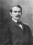
- American engineer Lee de Forest, 1904. www.widipedia.org
- As created by Lee de Forest, the first triode. www.widipedia.org
In de Forest’s triode, a mesh shaped “control grid” is placed between the cathode and the anode with the mesh holes allowing electrons to flow through.
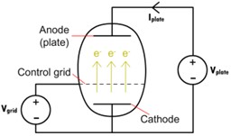
A simplified diagram of a vacuum tube triode. A small adjustment to the grid voltage has a comparatively large effect on the plate current, allowing the triode to be used for amplification. www.engineering.com
Adjusting the voltage applied to the control grid allows control of the number of electrons that can flow through the mesh from the cathode to the anode. A negative electrical potential (negative voltage) applied to the grid caused it to repel electrons, reducing electron flow to the anode, while increasing the control grid voltage allowed more electrons can pass through it.
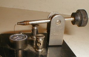
A “cat whisker detector”, using a fine metal wire in contact with a piece of galena (lead sulfide crystal) used in early crystal radio recalls Braun’s earlier discovery of metal-semiconductor junction effects.
www.wikipedia.org
Using this characteristic of a triode made it a useful signal amplifier, where a small change in the control grid voltage led to a large change in the electron flow to the anode. AND the triode could also work as an ON/OFF switch, just what was needed to control the“1”s and “0”s!
The development of transistors, and the Nobel Prize in Physics, would soon follow.
Now, instead of using mechanical or electro-mechanical switches to represent binary states, there were vacuum tube switches. While mechanical gears and relays operated in durations of milliseconds, vacuum tubes operated in microseconds. High volumes of data could now be stored, accessed, and processed at high speed: digital electronics had arrived!
But while the vacuum tube was a great leap forward in non-mechanical and non-electro-mechanical switches, knowledge of solid-state electronics, where there are no moving parts and not vacuum tubes, was also advancing. The beginnings of solid-state electronics can be traced back to the late 1800’s with the research and inventions around electric current flow associated with contacts between crystals and metal.
In 1874, Karl Ferdinand Braun, a German electrical engineer, first discovered that a point-contact metal-semiconductor junction could rectify, or convert, alternating current to direct current. He went on to build the first cathode-ray tube and cathode-ray oscilloscope (think television screens and earlier computer monitors!).
Eventually this led to work by John Bardeen and Walter Brattain in late 1947 at AT&T Bell Labs in New Jersey on the electrical signals produced between gold contacts and a germanium crystal. The output power of the signal produced in these experiments was more than the input signal, and this was the called the first “point-contact transistor”.
The word “transistor” means the combination of transfer and resistance, in which resistance is transferred from one end of the device to the other end. The vacuum tube had “transconductance,” which related to the current through the output of the device and the voltage across the device’s inputs. The transistor is its “dual”, relating the ratio between the voltage at the devices’ outputs and the current through its inputs. The word dual refers to these two terms, each being the flip side of the other, interchanging voltage and current.
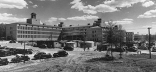
Bell Telephone Laboratories, Murray Hill, New Jersey, 1940’s. www.newprovidencehistorical.com
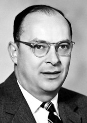
- John Bardeen, American physicist, 1956. www.wikipedia.org
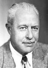
- Walter Houser Brattain, American physicist, 1950. www.wikipedia.org
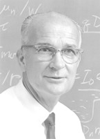
William Bradford Shockley was the Solid State Physics Group leader at Bell Labs, working with Bardeen and Brattain. Together these three jointly received the 1956 Nobel Prize in Physics for their semiconductor work and discovery of the transistor effect.
- William Shockley, American physicist, 1975. www.wikipedia.org
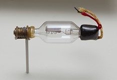
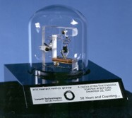
- Point-contact Transistor replica invented at Bell Labs in 1947. www.wikipedia.org
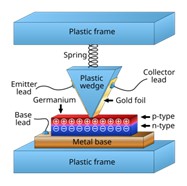
- Representation of the point-contact transistor (explained below). www.wikipedia.org
The point-contact transistor drawing above shows a gold foil split finely at the narrow point of a plastic wedge, forming two contacts very narrowly separated in contact with the p-type (positive) surface layer of a germanium crystal layer. This combined with other elements to form “holes” or “electron holes,” which is the absence of electrons where they would other be (see the image below). The base of the germanium is an n-type (negative) layer that has been combined with elements that donate electrons, with the 2 sections of gold foil forming the collector and emitter; the metal base has an electrode attached to form the base electrode.
The surface layer of the germanium contained an excess of electrons, but when an electric signal was passed through the thin gold foil it caused electron holes resulting in a thin surface layer with few electrons (the p-layer). When a low positive current is introduced to one of the two gold foil contacts (the emitter), it altered the current flowing between the other contact and the metal base on which the germanium was sitting. A relatively small change to the one contact current resulted in an even larger change in the second contact current between the metal base and the collector.
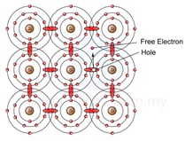
Representation of a crystal lattice of silicon showing a free electron resulting in an electron hole. www.spmphysics.com.my
This makes the transistor very useful as an amplifier, but could it be used as a switch?
The basic idea is that when there is no emitter current flow, the transistor is “off”, in the “0” state. If a current flow is applied to the emitter that is large enough to saturate the transistor, then the collector current would reach its maximum and produce the “on” or “1” state. At the saturation point, the collector current is as large as it can be, no matter how much higher the emitter current were to go. When the transistor is “on” the collector output is always the same, regardless of whether the single emitter input current is raised or if additional input currents are introduced.
Here we’re talking about very small amounts and variations in voltage and current, but enough to make the transistor effective.
As with the vacuum tube, the transistor can be used with the binary representation of symbols, numbers, and letters. Things became even better when transistors were combined and configured in various configurations, where multiple transistors can combine into a large transistor, inputs can come from multiple sources, and current flow can be inverted. This also enabled the creation of a range of logic gates now common to computing: OR, AND, NOT, and more.
But point-contact transistors proved difficult to manufacture reliably, it was an awkward construction of plastic, germanium, gold foil and a spring. Although they were used in some early computers their role became primarily for amplification with diodes providing logic in hearing aids, oscillators, telephone-routing gear, and in an experimental TV receiver. Soon, however, came another development: the bipolar junction transistor (BJT).
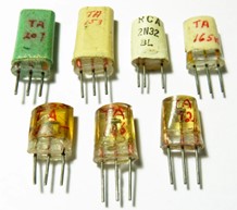
- Some point-contact transistors manufactured by RCA in 1953 for their experimental TV. Transistor Museum Jonathan Hope Collection. www.spectrum.ieee.org
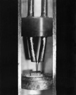
- The interior of a point-contact transistor, the two very thin conductors are the emitter and collector, sitting just in contact with the very small piece of germanium. A&T Archives and History Centre. www.sprectrum.ieee.org
But first a bit of gossip here.
Apparently, William Shockley was pretty upset when his name didn’t appear with Brattain’s and Bardeen’s on the original patent application for the point-contact transistor. Shockley believed that his theories had been the source of that work, despite having built his own transistor based on his theories which apparently didn’t work.
Well, indignant as he was, Shockley decided he’d had enough, and over the next few weeks in January and February 1948 he worked on his own new ideas for a transistor semiconductor “sandwich,” or perhaps more appropriately a wafer. The outer layers would be semiconductors with an abundance of electrons, and the area in the middle would have a deficiency of electrons. As the voltage on the middle area was changed it could turn on and off the current flow in the sandwich, meaning that electrons were traveling completely through the body of the semiconductor, not just along the surface!
When Shockley’s teams shared their findings on experiments with this new approach to the entire group, all were stunned, and none more so than Brattain and Bardeen who were totally unaware of the work Shockley had been doing. Gone was a spring forcing a gold-foiled wedge into the surface of a tiny block of semiconductor.
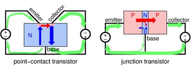
Comparative representation of a point-contact transistor and a bipolar junction transistors. ww.pa3fwm.nl
The development of semiconductors propelled the next steps.
And here the term “semiconductor” needs some explanation. It is a material with some of the properties of both insulators and conductors, with silicon being the most commonly used; germanium and gallium arsenide were alternatives. They can be manipulated to control electricity flow. By adding impurities, which is called doping, the conductivity of the material can also be altered. These properties make them useful in amplification applications, but also very importantly as switches, which again is what is needed in the digital binary world of “0”s and “1”s of computer electronics.
Below is a diagram of the point-contact transistor and the bipolar junction transistor.

The bipolar junction transistor (BJT) “sandwich” was a more straight forward, sturdier construction without springs forcing a gold-foiled wedge into the surface of the germanium. www.mks.com
The semiconductor material is coloured in blue or red with the N and P indicating n-type or p-type material. BJT’s uses two p-n junctions between two semiconductor types and uses both electron holes as well as electrons. One key point here is that point-contact transistors worked in “saturated current mode”, which slows things down because it takes time for the electrons and electron holes to decay when the transistor is switched. BJT’s are used in “voltage mode” rather than “saturated current mode,” and provide improved overall performance. They are also less finicky to produce, sturdier in construction, and more reliable overall.
Here are some examples of various manufactured BJT’s.
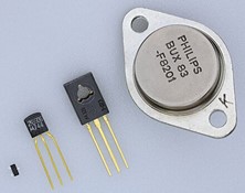
Some typical individual BJT sandwich/wafer designs. Manufacturing capabilities and techniques had much improved. www.wikipedia.org
Even more progress occurred with the development of the field-effect transistor (FET), which used an electric field to control the current through a semiconductor. When a voltage is applied to the gate, it will alter the conductivity between the drain and the source, and FETs can use either electrons or electron holes as charge carriers. Since a transistor’s collector current (see the image below) is proportionally limited by its base current (see gate image below), it can be used as a type of current-control switch (with the emitter being analogous to the source below).
And again, because the FET can act as switch, it is well suited to binary world of digital electronics. FETs also offer several advantages including low power consumption, high input impedance, and simple biasing (steady DC current or voltage) requirements.
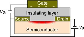
Drawing of conventional field-effect transistor (FET). Positive (+) and negative charges are accumulated on a semiconductor channel and a gate electrode, respectively, by applying a gate voltage V(G). www.researchgate.net
As well, FETs have many variations, including the junction field-effect transistor (JFET), the status induction transistor (SIT), the metal-oxide-semiconductor FET (MOSFET), and the complementary metal oxide semiconduction (CMOS).
Of all the various types of FETs, the MOSFET (also invented at Bell Labs between 1955 and 1960) is the most common.
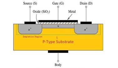
N-Channel Type MOSFET. www.hackatronic.com
The first digital integrated circuits ushered in the modern computing age.
Also, using MOSFETs eventually enabled the development of complementary metal oxide semiconductor (CMOS) fabrication process technology which is at the heart of what we call digital integrated circuits (digital IC’s, IC’s or “chips”). CMOS fabrication process technology is all about using symmetrical and complementary pairs of MOSFETs to build digital logic capabilities in chips including memory chips, microprocessors, microcontrollers, and basic input/output (BIOS) firmware chips.
Today’s integrated circuits combine millions or billions of MOS-type transistors. Typically, they are composed of silicon wafers made up of many overlapping layers, each demarcated using photolithography for doping or for deposits of various materials, insulators or metals and then etched to produce all of the electronic components required, such as transistors, capacitors, and resistors. Current precision manufacturing techniques and technology allows billions of these components on very small sized chips, which brings us back to the quote from Gordon Moore at the beginning of this article:
“The number of transistors and resistors on a chip doubles every 24 months.” — Gordon Moore
While it is commonly referred to as “Moore’s law”, it isn’t really a law but instead an observation and projection based on data collected from about 1970 to approximately current times. To incorporate more and more transistors in an integrated circuit requires that semiconductor devices get smaller and smaller. For example, currently IBM’s 2 nanometer chip technology places about 50 billion transistors, each the size of approximately 5 atoms, on a chip about “the size of a human fingernail.” Consider that: a strand of human DNA is 2.5 nanometers, and that atoms and quarks are both smaller than a nanometer (from 0.1 to 0.5 nanometers).
So how likely is it that transistors can be made that are smaller than atoms? The size of a silicon atom is 0.2 nanometers, so silicon-based transistors can’t get smaller than that. Perhaps bismuth, which is a semi-metal, could be used; after all silicon was selected as a semiconductor material because it’s the second most common element found on the periodic table. But the smaller the chip, the more complex it is to make them – and how can heat effectively dissipate as more and more transistors are crammed into a smaller space?
What does the future hold?
Maybe transistors aren’t the future, and the use of quantum bits (qubits) in quantum computers will entirely change computing technology. For example, qubits could be made from trapped ions, photons, artificial or real atoms, or quasiparticles.
Or perhaps carbon nanotubes, which are molecules in the form of a hollow cylinder of pure carbon about a nanometer in diameter, will replace silicon.
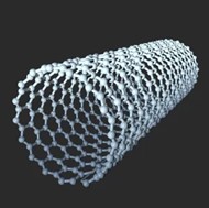
Illustration of a carbon nanotube. www.britannica.com
Let’s remember and celebrate the progress we’ve already made, from human “computors” to the vacuum tube, transistors, and integrated circuit chips.
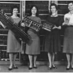
- Human “computors” display the first four programming boards. From left: Patsy Simmers with ENIAC board; Gail Taylor with EDVAC (Electronic Discrete Variable Automatic Computer) board; Milly Beck with ORDVAC (Ordnance Discrete Variable Automatic Computer) board; Norma Stec with BRLESC-1 (Ballistic Research Laboratories Electronic Scientific Computer-1) board. From vacuum tubes to transistors. National Museum, United States Army. www.thenmusa.org
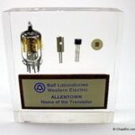
- Bell Labs “Transistor History” vacuum tube, point-contact transistor, bipolar junction transistor, integrated circuit chip www.chipsetc.com
And in 1995, a group at the University of Pennsylvania reproduced the beloved ENIAC on a chip!
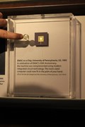
ENIAC on a Chip, University of Pennsylvania (1995) – Computer History Museum.
www.wikipedia.org
But that was in 1995. In 2023 when Apple released the A17 processor it had about 19 billion transistors!
“If you built an iPhone with vacuum tubes instead of transistors, packed together with the same density as they were in UNIVAC, the phone would be about the size of five city blocks when resting on one edge. Conversely, if you built the original UNIVAC out of iPhone-size components, the entire machine would be less than 300 microns tall, small enough to embed inside a single grain of salt.” — Randall Munroe, Additional Serious Scientific Answers to Absurd Hypothetical Questions
These are impressive achievements, all built on fundamental scientific principles and theories, research, experiments, discoveries, and development that occurred many decades ago.
The discovery of the diode can be traced to German physicist Ferdinand Braun in 1874 and John Ambrose Fleming’s diode patented in 1904. Lee de Forest’s invention of the first three-electrode tube (the triode) occurred in 1907. In 1925 Julius Edgar Lillenfield first patented the basic principle of the field-effect transistor. In 1934 Oskar Heil independently patented a similar device in Europe in 1934. Bardeen, Brattain and Shockley attempted to build a field-effect device at Bell Labs in the 1940s which directly led to their discovery of the transistor effect for which they were awarded the Nobel Prize. But even though there have been incredible advances in engineering and related manufacturing processes, still today the MOSFET remains the predominant transistor type in digital electronics.
Early devices might not have looked elegant or impressive but look closely and you’ll see how today’s world of electronics all began.
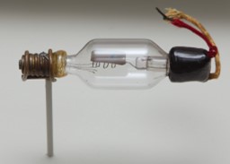
The first triode, the de Forest Audion, invented 1906.
www.historyofinformation.com
Your feedback helps us shape The Quantum Record just for you. Share your thoughts in our quick, 2-minute survey!
☞ Click here to complete our 2-minute survey

